PCB laser processing services
Much of the printed circuit board (PCB) work done in the USA is quick turn around or prototype design, including laser skiving. These processes are well suited to the laser’s flexibility and accuracy. This work is mainly a combination of IR and UV lasers. Accu-Tech Laser Processing has long been a ‘Go To’ company when it comes to laser cutting PCBs and various laser skiving for the electronics industry. Our many years of experience with multiple laser types help us solve your design requirements. Check our About Us info to see more about our offerings for de-paneling, micro via drilling, and laser skiving! Check out our Capabilities and Materials page to see the materials that we routinely process in our PCB department.
To see what’s happening in the Microelectronics world visit the iMAPS website.
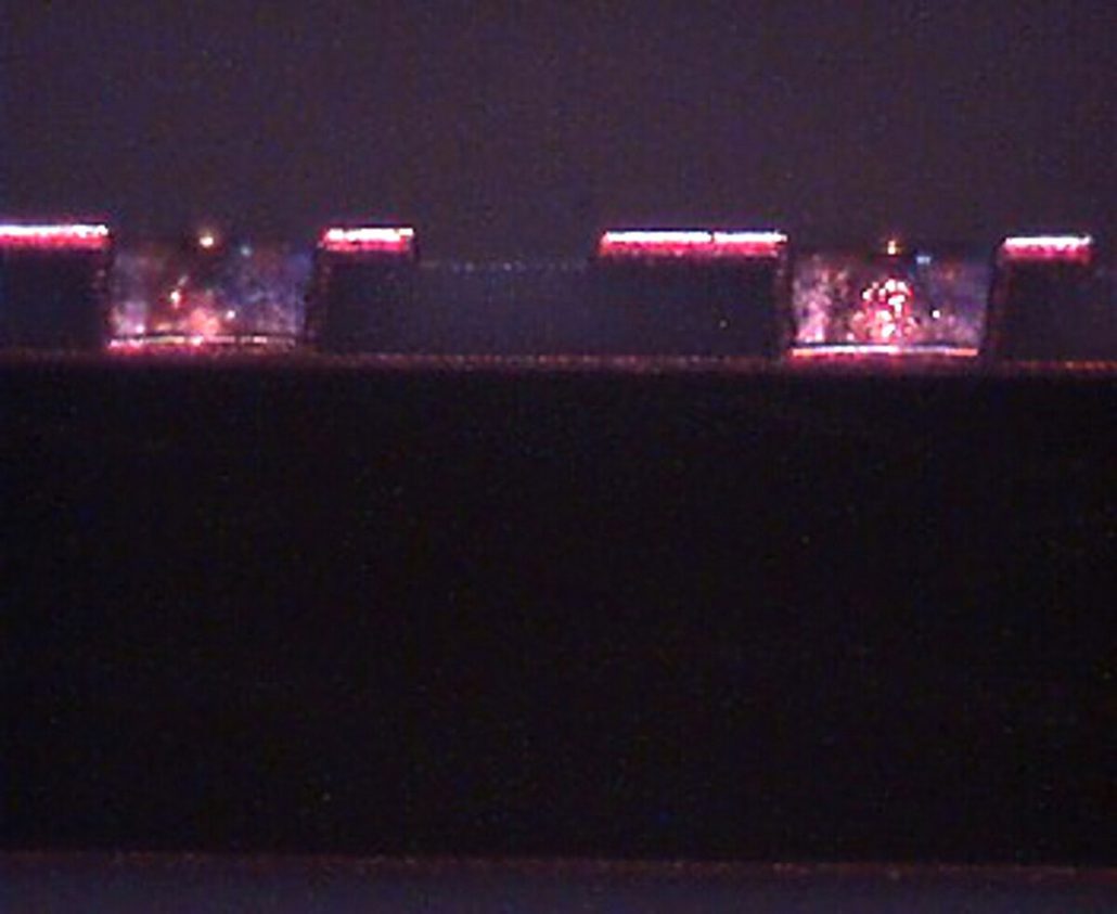
A cross-section of plated Mircro-Via. Vias are typically .006″ diameter going through .002-.003″ thick dielectric. Furthermore, the top layer of copper can either be solid copper or pre-etched with the desired via diameter and locations. Also, these PCBs may have a few hundred vias or more than 100k vias per side.
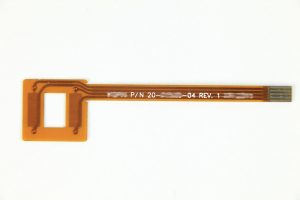
Flex Circuit singulation or profiling. Accu-Tech’s laser systems allow optically aligning to existing patterns and laser routing/singulation of flex circuits. Laser routing is often much more appropriate for prototype quantities due to reduced fixturing costs.
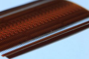
Laser Skiving to expose Flying Leads beneath polyimides or coverlay materials. Our lasers can clean up excess adhesive squeeze out due to lamination as well as excess solder mask on PCBs.


