Capabilities and Processes:
Laser processing adds value to your product as well as aid in manufacturing steps and benefits design.
Various Laser capabilities are listed below.
Cutting (machining) of features or outer profiles –
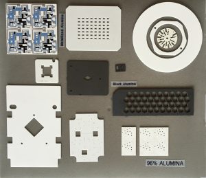
Your design is easily converted to a precise computer controller motion file by our CAM software. Laser machining is sometimes the only option for extremely hard materials such as alumina ceramics. Hardness or softness is not a limiting factor for the laser. The small laser beam diameter adds flexibility to your design. Furthermore, easy to prepare ‘soft tooling’ saves time and money over conventional tooling. The laser beam does not wear out from contact with materials – This is true for one or two prototypes up to thousands of parts.
This laser processing can be done on blank materials or precisely aligned with your pre-existing features.
Drilling (often applied to producing round holes) can be used for reducing weight, providing through paths for electrical connections or component pins. Drilling can provide clearance for parts in stack-ups.
Scribing is generally done on ceramics. This is a lower cost complement to laser machining. Laser scribing usually generates arrays of circuit boards ready for thick film printing and later separation (snapping by hand or automatic roll or guillotine breaker). Finished part size control is not quite as tight as with laser machining but scribing is a less expensive process.
Modification
Ablating can cleanup or remove excess material left from epoxy squeeze out or remove a polymer layer down to an existing metal layer without damaging the metal. Solder masks can be removed in areas that require access to an electrical pad inadvertently covered.
Marking serial numbers or part numbers onto components gives permanent traceability for your Quality system. Marking can also aid component positioning on a circuit board or act as a solder dam restricting flow to particular areas.
Singulating or separating of individual parts produced in arrays is easy with laser. Workstations have high magnification video cameras for accurate registration to existing reference marks. Computer systems can correct for shrinkage or expansion of parts or arrays due to previous manufacturing steps.
Tabbed in arrays – Accu-Tech can produce your part in an array, each part held into the array by a set of tabs or straps giving you a group of parts for subsequent processing a single unit for increased throughput. Ceramic substrates and flexible polymer panels are often produced this way.
Micro vias – blind vias – are the workhorse of the PCB industry. Small holes produced through one layer of copper through a dielectric layer down to another copper layer. These holes are usually less than .008” (.2mm) in diameter. A PCB layer may have from a few hundred to over one hundred thousand micro-vias. These holes are produced several hundred per second by laser.
Welding
Welding or micro-welding on many metals – spot welds or seam welds will stake components in place. Inert cover gases are available if required for the application.
Post alignment – Laser work aligned to preexisting features on ‘Customer Supplied’ materials. Much of the work performed by Accu-Tech Laser Processing is done in this manner. We understand our responsibility to care for the materials entrusted to us for laser work.

